
Science. For you.
Transmission Electron Microscopy (TEM)
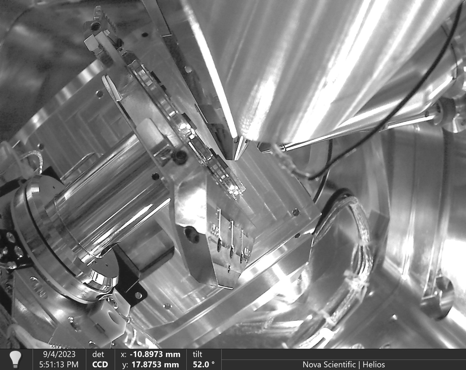
-
TEM Imaging
Micro structure characterization.
Thickness of TEM sample should be below 100nm.
Diffraction spot shows 3D crystal structure of material in atomic scale.
(4Co-750C-24h)

-
HR-TEM Imaging
Thickness of sample is between 30nm to 70nm.
Morphology characterization of 2D atom arrangement.
Dislocation or twin crystal structure can be observed
(4Co-750C-24h)

-
TEM-EDS Analysis
Obtain component information and qualitative analysis through X-ray.
Points, line or map element measurement.
Nano scale accuracy.
(4Co-750C-6h)